
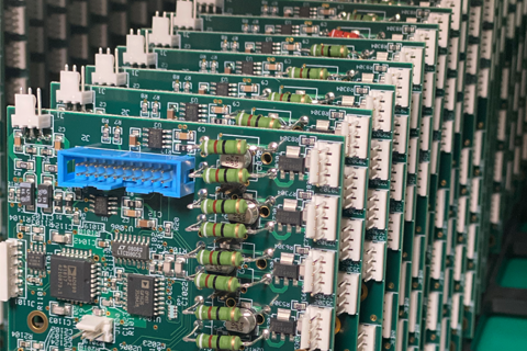
Processes involved in PCB assembly
PCB assembly involves a number of processes, including picking and placing components, applying solder paste, soldering, and testing. Most PCB assembly processes use surface mount technology. To begin, the board is cleaned and drilled. Once the board is clean, it is then coated with a thin layer of copper. This process allows the board to be tested and inspected for quality.Once the raw circuit boards have been ordered, the PCB contract manufacturer (CM) will choose a fabricator whose capabilities match the project’s technical requirements. Once a PCB CM has selected a fabricator, the manufacturer will proceed to the fabrication stage. It is important to ensure that the PCB fabrication vendor has a separate production line for prototype boards. In addition, prototype PCB fabricators will conduct design reviews using Gerber data.Techniques used to apply solder paste
There are several different techniques used to apply solder paste to a PCB assembly. Some of them are simple and can be done at home. The stenciling technique, for example, can be used to apply solder paste to the pads of a circuit board. It is important to use the correct amount of paste. Applying too little can create weak joints. Applying too much can cause large joints, as well as shorts between adjacent pads.Solder paste has a viscosity, or resistance, that depends on the metal content. The higher the metal content in the solder paste, the higher its viscosity. The higher the temperature, the lower the paste’s viscosity. Solder pastes are also characterized by their Rheology, which determines their flow characteristics. The correct amount of solder paste can result in a strong and even solder joint.Tools used to inspect solder paste layers
Solder paste inspection is an important process in PCB assembly. It allows you to detect defects and ensure that the solder paste layer is of high quality. This process can be manual or machine-based. Automated inspection can reduce costs incurred by rework. It can also improve production efficiency by identifying poor solder paste printings.During the PCB assembly process, solder paste is applied to the printed circuit board by using stencils. These stencils are made of stainless foils and are used to ensure the proper application of solder paste. The stencils also act as solder masks to prevent over-deposition of solder paste. The electrical components are then attached to the PCB using a soldering machine. Lead or tin solder is used to adhere the components to the board.Identifying test points on a PCB
Testing your circuit board is essential to the success of your project. There are several methods you can use to test the components on your board. The easiest method is to measure the resistance of the components using a multimeter. However, it is important to know both ends of the component so that you can accurately interpret the test results.Before you start designing your PCB, you should consider the test points that will be required. These may be component pads, vias, or printed elements. To test the components, you need a multimeter and a multi-digit ohm meter.Testing for defects
Testing a PCB assembly for defects is crucial for the quality of the finished product. The assembly process is highly complex and involves many different processes and components. These processes can introduce defects into the finished product without the engineer’s knowledge. This means that testing a PCB is a challenging job. To ensure that your PCBs are defect-free, you should employ a failure-proof testing strategy.PCB assembly testing includes a series of visual, functional and electrical tests. Popular PCB assembly testing methods include automated optical inspection, X-ray imaging, and in-circuit testing. A comprehensive test of the assembled PCB will reveal whether there are any defects in the design, fabrication, or soldering processes.Yasir Asif has expertise in SEO and digital marketing.